2D Materials | Complex Oxides | Defects | Porous Materials | Nanocrystals | Electronic Orbitals | Theory & Simulations
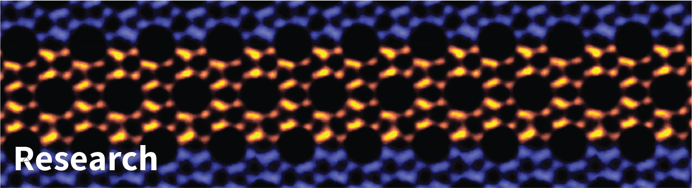
2D Materials
Several atomic-layer-thick materials, often referred to as "two-dimensional" (2D) materials have substantially changed the landscape of nanotechnology because of their extraordinary mechanical and electrical properties. For example, graphene, which exists as a single layer of carbon atoms, possesses a tensile strength 300 times larger than that of commercial steel and transports electric charges over an order of magnitude faster than silicon.
Our 2D material research[1-4] combines analytical scanning transmission electron microscopy (STEM) and theoretical modeling of electron-material interactions to elucidate unambiguously the atomic, chemical, and electronic structure of novel 2D materials. This research aims to improve the understanding of 2D materials’ enhanced properties as well as aid in their synthesis and device application. We study a variety of 2D material systems ranging from black Phosphorus and black Arsenic as well as Van der Waals materials systems such as MoS2, CrTex, etc.
Recommended Reading
-
"Layer Dependence of Dielectric Response and Water-Enhanced Ambient Degradation of Highly Anisotropic Black As" H. Yun, S. Ghosh, P. Golani, S. J. Koester, K. A. Mkhoyan - ACS Nano. 14, 5988 (2020)
-
"Atomic-resolution analytical scanning transmission electron microscopy of topological insulators with a layered tetradymite structure" D. Reifsnyder Hickey, K. A. Mkhoyan - APL Mater. 8, 070902 (2020)
-
"Van der Waals contacts between three-dimensional metals and two-dimensional semiconductors" Y. Wang, J. C. Kim, R. J. Wu, J. Martinez, X. Song, J. Yang, F. Zhao, K. A. Mkhoyan, H. Y. Jeong, M. Chhowalla; Nature 568, 70 (2019) Highlighted in C&EN.
-
"Room-temperature high spin-orbit torque due to quantum confinement in sputtered BixSe(1–x) films" M. DC, R. Grassi, J. Y. Chen, M. Jamali, D. Reifsnyder Hickey, D. Zhang, Z. Zhao, H. Li, P. Quarterman, Y. Lv, M. Li, A. Manchon, K. A. Mkhoyan, T. Low, J. P. Wang; Nature Mater. 17, 800 (2018) Highlighted in Nature Materials News & Views
-
"Atomic and electronic structure of exfoliated black phosphorus" R. J. Wu, M. Topsakal, T. Low, M. C. Robbins, N. Haratipour, J. S. Jeong, R. M. Wenzcovitch, S. J. Koester, K. A. Mkhoyan - J. Vac. Sci. Technol. A 33, 060604 (2015). [Ed. Pick] Highlighted on JVSTA Cover.
-
"Atomic and Electronic Structure of Graphene-Oxide" K.A. Mkhoyan, A.W. Contryman, J. Silcox, D.A. Stewart, G. Eda, C. Mattevi, S. Miller, M. Chhowalla - Nano Lett. 9, 1058 (2009).
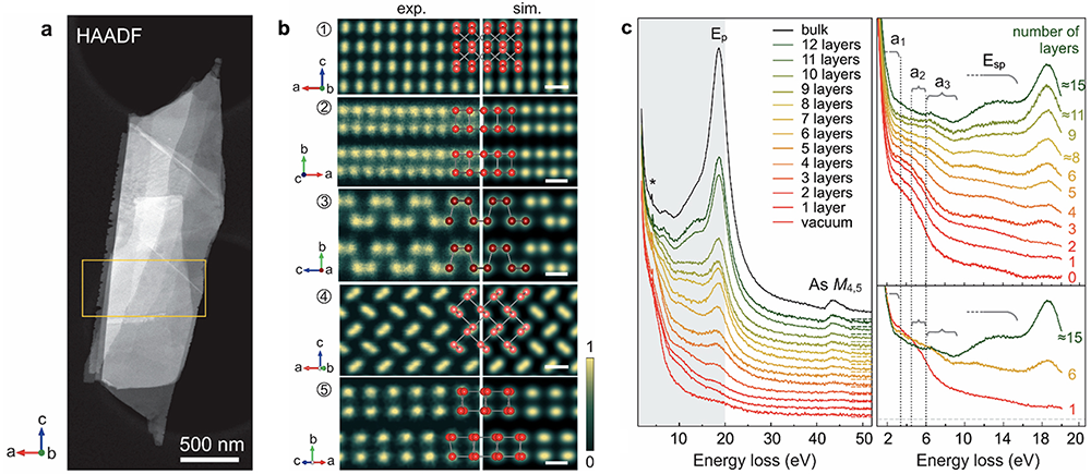
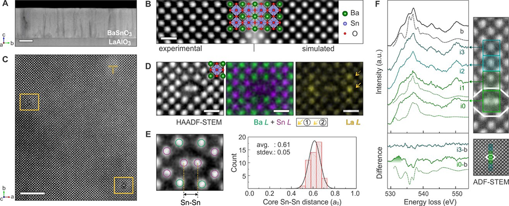
Complex Oxides
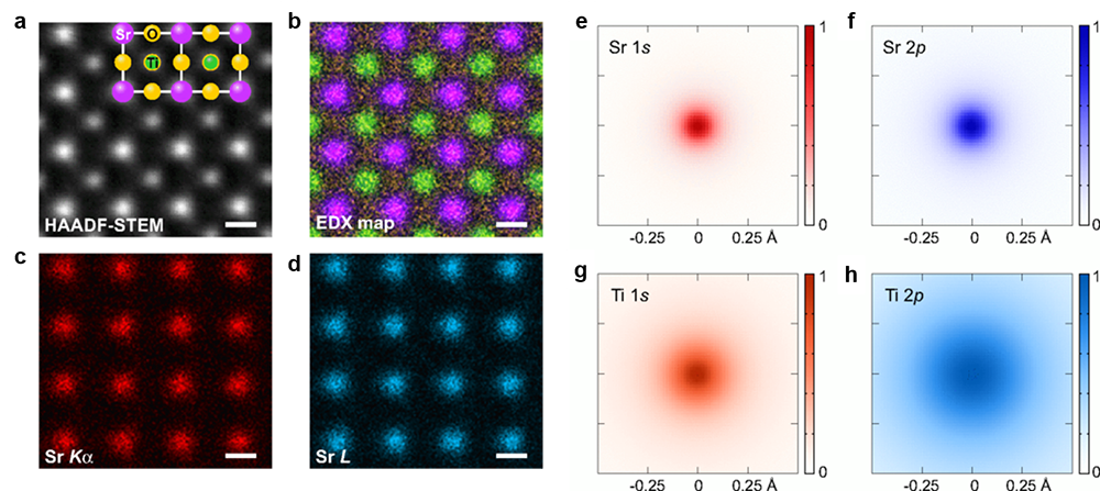
Our research interest is to reveal the atomic and electronic structure of the perovskite structure complex oxide using high-angle annular dark-field (HAADF) scanning transmission electron microscope (STEM) and analytical TEM (transmission electron microscope.) Local atomic structures are observed at sub-angstrom resolution and the electronic structure of characteristic atomic structures is investigated by interpreting EELS (electron energy loss spectroscopy) spectra.
Recommended Reading
-
"Dopant Segregation Inside and Outside Dislocation Cores in Perovskite BaSnO3 and Reconstruction of the Local Atomic and Electronic Structures" H. Yun; A. Prakash; T. Birol; B. Jalan, K. A. Mkhoyan - Nano Lett., 21, 10, 4357–4364 (2021)
-
"Metallic line defect in wide-bandgap transparent perovskite BaSnO3" H. Yun, M. Topsakal, A. Prakash, B. Jalan, J. S. Jeong, K. A. Mkhoyan - Sci. Adv. 7, eabd4449 (2021)
-
"Self-Assembled Periodic Nanostructures Using Martensitic Phase Transformations" A. Prakash, T. Wang, A. Bucsek, T. K. Truttmann, A. Fali, M. Cotrufo, H. Yun, J. Kim, P. J. Ryan, K. A . Mkhoyan, A. Alu, Y. Abate, R. D. James, B. Jalan - Nano Lett., 21, 3, 1246–1252 (2020)
-
"Microstructure characterization of BaSnO3 thin films on LaAlO3 and PrScO3 substrates from transmission electron microscopy" H. Yun, K. Ganguly, W. Postiglione, B. Jalan, C. Leighton, K. A. Mkhoyan, J. S. Jeong - Sci Rep. 8, 10245 (2018)
-
"A New Line Defect in NdTiO3 Perovskite" J. S. Jeong, M. Topsakal, P. Xu, B. Jalan, R. M. Wentzcovitch, K. A. Mkhoyan - Nano Lett. 16, 6816 (2016)
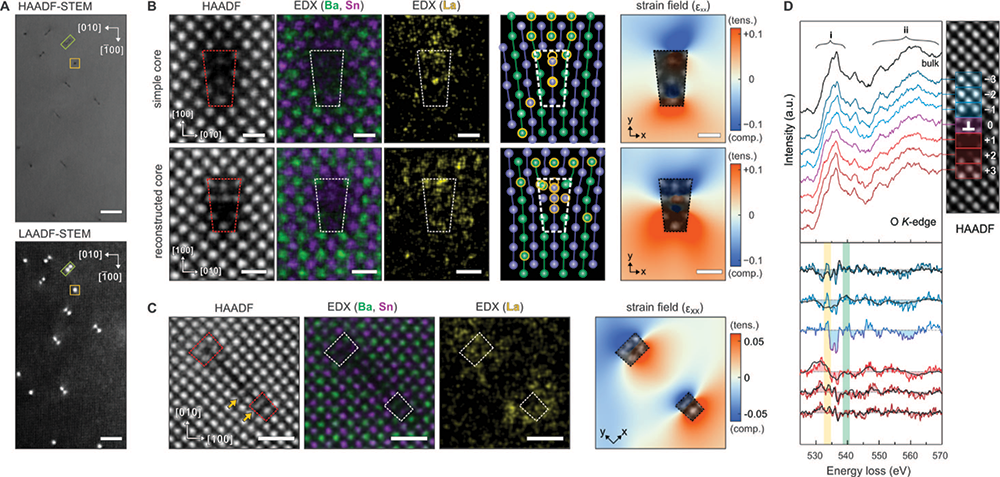
Defects
Defects at the atomic scale can be used to tune materials properties, with these imparting desirable properties in the relevant systems of interest such as enhanced membrane separation characteristics for zeolites and metallic behaviors in a typically insulating material. Our research interest focused on studying such defects in a variety of material systems such as 2D materials, perovskite oxides, porous materials, and molecular crystals, with a focus on identify/discovering new defects supported by detailed atomic structure characterization as well as chemical and electronic structure using a combination high-angle annular dark-field (HAADF) scanning transmission electron microscope (STEM) imaging and energy dispersive spectroscopy (EDX) and EELS in an analytical TEM (transmission electron microscope.)
Recommended Reading
-
"Metallic line defect in wide-bandgap transparent perovskite BaSnO3" H. Yun, M. Topsakal, A. Prakash, B. Jalan, J. S. Jeong, K. A. Mkhoyan - Sci. Adv. 7, eabd4449 (2021)
-
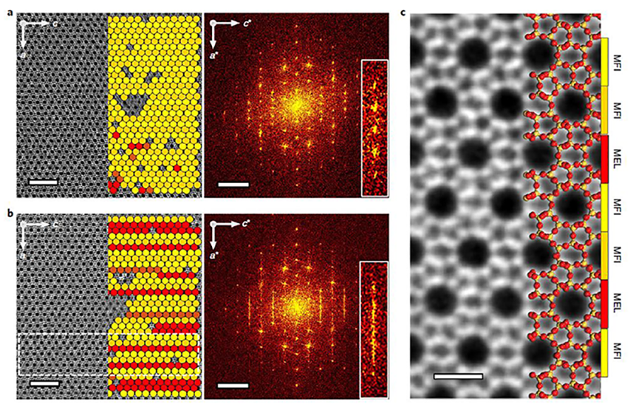
"One-dimensional intergrowths in two-dimensional zeolite nanosheets and their effect on ultra-selective transport" P. Kumar, D. W. Kim, N. Rangnekar, H. Xu, E. O. Fetisov, S. Ghosh, H. Zhang, Q. Xiao, M. Shete, J. I. Siepmann, T. Dumitrica, B. McCool, M. Tsapatsis, K. A. Mkhoyan; Nature Mater. 19, 443 (2020)
-
"Structure and basal twinning of topological insulator Bi2Se3 grown by MBE onto crystalline Y3Fe5O12" D. Reifsnyder Hickey, J. G. Azadani, A. R. Richardella, J. C. Kally, J. S. Lee, H. Chang, T. Liu, M. Wu, N. Samarth, T. Low, and K. A. Mkhoyan - Phys. Rev. Mater. 3, 061201(R) (2019)
-
"A New Line Defect in NdTiO3 Perovskite" J. S. Jeong, M. Topsakal, P. Xu, B. Jalan, R. M. Wentzcovitch, K. A. Mkhoyan - Nano Lett. 16, 6816 (2016)
Porous Materials
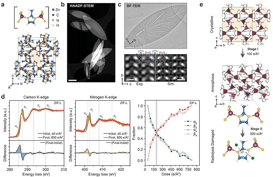
Porous materials metal-organic frameworks (MOFs) and zeolites are used in applications such as catalysis and separations. Low-dielectric constants as well as recently found conducting properties in MOFs make them attractive building blocks for electronic devices. To realize these applications, the structure and chemistry of MOFs at the atomic level needs to be explored and, in many instances, it should be done by direct observations. We used analytical scanning transmission electron microscopy (STEM) to study these materials down to the atomic level accompanied with chemical and electronic structure information using spectroscopic methods like energy dispersive X-ray (EDX) and electron energy-loss spectroscopy (EELS). As a result, it can provide a direct correlation between structure and properties. These STEM-based methods however rely on the interaction of high-energy electrons of the probe with MOF specimens, which can alter the structure of the materials. This is particularly challenging for MOFs that can handle only 1-102 e/Å2 dose of electrons (or just a few seconds of beam exposure). Hence, our focus is to establish STEM-based atomic-level analysis of beam-sensitive materials by (1) understanding the fundamentals of electron-beam irradiation on these systems and (2) develop new STEM-based techniques where atomic-resolution analysis can be reliably performed. The development of such techniques will open new avenues for direct imaging and characterizations of the local structure and chemistry of imperfections (point, line, and planar defects) in MOFs and zeolites as well as extend this to the molecular organic crystals.
Zeolites
Metal Organic Frameworks
Recommended Reading
-
"Two Distinct Stages of Structural Modification of ZIF-L MOF under Electron-Beam Irradiation" S. Ghosh, H. Yun, P. Kumar, S. Conrad, M. Tsapatsis, K. A. Mkhoyan - Chem. Mater., 33, 14, 5681–5689 (2021)
-
"Few-Unit-Cell MFI Zeolite Synthesized using a Simple Di-quaternary Ammonium Structure-Directing Agent" P. Lu, S. Ghosh, M. D. de Mello, H. S. Kamaluddin, X. Li, G. Kumar, X. Duan, M. Abeykoon, J. A. Boscoboinik, L. Qi, H. Dai, T. Luo, S. Al-Thabaiti, K. Narasimharao, Z. Khan, J. D. Rimer, A. T. Bell, P. Dauenhauer, K. A. Mkhoyan, M. Tsapatsis - Angew. Chem. Int. Ed., 60, 2–10 (2021)
-
"One-dimensional intergrowths in two-dimensional zeolite nanosheets and their effect on ultra-selective transport" P. Kumar, D. W. Kim, N. Rangnekar, H. Xu, E. O. Fetisov, S. Ghosh, H. Zhang, Q. Xiao, M. Shete, J. I. Siepmann, T. Dumitrica, B. McCool, M. Tsapatsis, K. A. Mkhoyan - Nature Mater. 19, 443 (2020)
-
"Ultra-selective high-flux membranes from directly synthesized zeolite nanosheets" M. Y. Jeon, D. Kim, P. Kumar, P. S. Lee, N. Rangnekar, P. Bai, M. Shete, B. Elyassi, H. S. Lee, K. Narasimharao, S. N. Basahel, S. Al-Thabaiti, W. Xu, H. J. Cho, E. O. Fetisov, R. Thyagarajan, R. F. DeJaco, W. Fan, K. A. Mkhoyan, J. I. Siepmann, M. Tsapatsis - Nature 543, 690 (2017)
-
"Open-Pore Two-Dimensional MFI Zeolite Nanosheets for the Fabrication of Hydrocarbon-Isomer-Selective Memberanes on Porous Polymer Supports" H. Zhang, Q. Xiao, X. Guo, Najun Li, P. Kumar, N. Rangnekar, M. Jeon, S. Al-Thabaiti, K. Narasimharao, S. N. Basahel, B. Topuz, F. J. Onorato, C. W. Macosko, K. A. Mkhoyan, M. Tsapatsis - Angew. Chem. Int. Ed. 55, 7184 (2016)
Nanocrystals
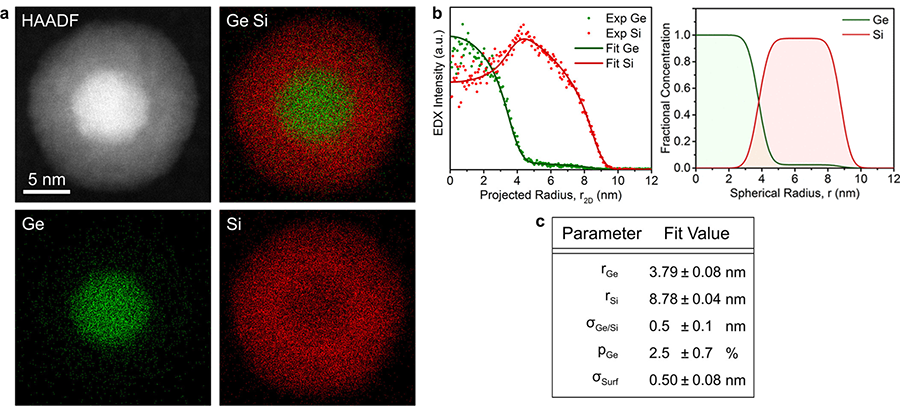
Nano-scale particles (0-100 nm) of many materials exhibit unique properties that are very distinct from their bulk behavior such as catalytic activity and optoelectronic properties. The ability to reliably manipulate these properties on the nanometer scale has made nanocrystals extremely important in a wide variety of fields from bioimaging to high-performance catalysts, to television screens. The key to harnessing and manipulating the properties of nanocrystals lies in the fine and reliable control of size, shape, and composition. In our lab, we analyze these characteristics of individual nanocrystals using scanning transmission electron microscopy paired with spectroscopy techniques such as energy dispersive X-ray (EDX) spectroscopy and electron energy loss (EEL) spectroscopy. With these tools, we are able to directly observe individual dopant atoms, characterize interfaces between layers of materials in core/shell nanocrystals, and evaluate the shape and structure of individual nanocrystals with a resolution well beyond the reach of other characterization techniques.
Recommended Reading
-
"Obtaining Structural Parameters from STEM-EDX Maps of Core/Shell Nanocrystals for Optoelectronics" J. T. Held, K. I. Hunter, N. S. Dahod, B. L. Greenberg, D. Reifsnyder Hickey, W. A. Tisdale, U. R. Kortshagen, and K. A. Mkhoyan - ACS Appl. Nano Mater. 1, 989 (2018)
-
"Nonthermal Plasma Synthesis of Core/Shell Quantum Dots: Strained Ge/Si Nanocrystals" K. I. Hunter, J. T. Held, K. A. Mkhoyan, U. R. Kortshagen - ACS App. Mater. Interfaces 9, 8263 (2017)
-
"Nonequilibrium-Plasma-Synthesized ZnO Nanocrystals with Plasmon Resonance Tunable via Al Doping and Quantum Confinement" B. L. Greenberg, S. Ganguly, J. T. Held, N. J. Kramer, K. A. Mkhoyan, E. S. Aydil, U. R. Kortshagen - Nano Lett. 15, 8162 (2015)
-
"High electron mobility in thin films formed via supersonic impact deposition of nanocrystals synthesized in nonthermal plasmas" E. Thimsen, M. Johnson, X. Zhang, A. J. Wagner, K. A. Mkhoyan, U. R. Kortshagen, E. S. Aydil - Nature Commun. 5, 5822 (2014).
-
"Imaging 'Invisible' Dopant Atoms in Semiconductor Nanocrystals" A. A. Gunawan, K. A. Mkhoyan, A. W. Wills, M. G. Thomas, D. J. Norris - Nano Lett. 11, 5553 (2011). Highlighted in Nature Chemistry.
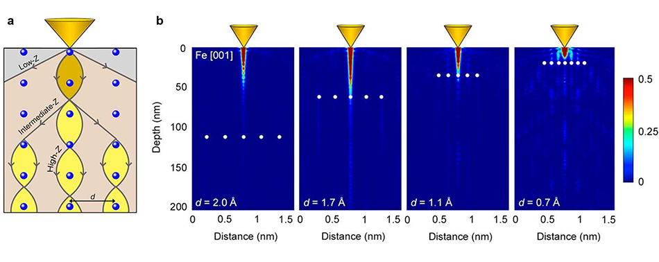
In order to quantitatively analyze atomic resolution experimental images from a transmission electron microscope, it is crucial to fully understand and account for the many complex interactions between the beam and the specimen. Therefore, we dedicate considerable effort to simulating electron microscope images from the first principles for comparison with experimental data. By matching our experimental work with analogous simulations, we are able to accurately determine specimen thickness, structure, and orientation, observe the effects of bonding between atoms and determine the positions of individual dopant atoms. Through such work, we are advancing the field of electron microscopy and finding new ways of characterizing material behavior at atomic resolution.
Electronic Orbitals
While we know that all matter is composed of atoms, our understanding of the electron orbitals that are fundamental to the properties of these atoms has historically been limited to theory and indirect evidence rather than direct experimental measurements of electron density. Work in x-ray diffraction, electron diffraction, and transmission electron microscopy have produced maps of electron densities in near-defect-free crystals. Additionally, atomic force microscopy and scanning tunneling microscopy have been used to characterize bonding electron orbitals of individual molecules and surface atoms. Our work has focused on directly characterizing core-level electron orbitals using spatially resolved energy-dispersive x-ray spectroscopy (EDX) in a scanning transmission electron microscope (STEM).
Recommended Reading
-
"Probing core-electron orbitals by scanning transmission electron microscopy and measuring the delocalization of core-level excitations" J. S. Jeong, M. L. Odlyzko, P. Xu, B. Jalan, and K. A. Mkhoyan - Phys. Rev. B 93, 165140 (2016)
-
"Atomic bonding effects in annular dark field scanning transmission electron microscopy. II. Experiments" M. L. Odlyzko, J. T. Held, K. A. Mkhoyan - J. Vac. Sci. Technol. A 34, 041603 (2016). [Ed. Pick]
-
"Atomic bonding effects in annular dark field scanning transmission electron microscopy. I. Computational predictions" M. L. Odlyzko, B. Himmetoglu, M. Cococcioni, K. A. Mkhoyan - J. Vac. Sci. Technol. A 34, 041602 (2016). [Ed. Pick]
-
"Improving Signal-to-Noise Ratio in Scanning Transmission Electron Microscopy Energy-Dispersive X-Ray (STEM-EDX) Spectrum Images Using Single-Atomic-Column Cross-Correlation Averaging" J. S. Jeong, K. A. Mkhoyan - Microsc. Microanal. 22, 536 (2016)
Theory & Simulations
In order to quantitatively analyze atomic resolution experimental images from a transmission electron microscope, it is crucial to fully understand and account for the many complex interactions between the beam and the specimen. Therefore, we dedicate considerable effort to simulating electron microscope images from first principles for comparison with experimental data. By matching our experimental work with analogous simulations, we are able to accurately determine specimen thickness, structure, and orientation, observe the effects of bonding between atoms and determine the positions of individual dopant atoms. Through such work, we are advancing the field of electron microscopy and finding new ways of characterizing material behavior at atomic resolution.
Also, quantitative analysis of atomic resolution STEM images often requires the comparison of experimental data with simulations of beam propagation through and images of hypothesized structures. This, in turn, necessitates a thorough understanding of the phenomena that govern interactions of the STEM probe with a sample. Through first-principles simulation of the interaction between electrons in STEM probes with atoms in a variety of samples, we gain deeper insight into the root causes of observed phenomena. Results from this work can then be used to formulate hypotheses for new ways of characterizing specimens.
Recommended Reading
-
"STEM beam channeling in BaSnO3/LaAlO3 perovskite bilayers and visualization of 2D misfit dislocation network" H. Yun, A. Prakash, B. Jalan, J. S. Jeong, K. A. Mkhoyan - Ultramicroscopy 208, 112863 (2020)
-
"Sub-Atomic Channeling and Helicon-Type Beams in SrTiO3" J. S. Jeong, H. Song, J. T. Held, K. A. Mkhoyan - Phys. Rev. Lett. 122, 075501 (2019)
-
"Simplifying Electron Beam Channeling in Scanning Transmission Electron Microscopy (STEM)" R. J. Wu, A. Mittal, M. L. Odlyzko, K. A. Mkhoyan - Microsc. Microanal. 23, 794 (2017)
-
"Atomic bonding effects in annular dark-field scanning transmission electron microscopy. I. Computational predictions" M. L. Odlyzko, B. Himmetoglu, M. Cococcioni, K. A. Mkhoyan - J. Vac. Sci. Technol. A 34, 041602 (2016).
-
"Limits in detecting an individual dopant atom embedded in a crystal" A. Mittal and K. A. Mkhoyan - Ultramicroscopy, 111, 1101 (2011).